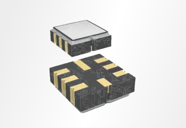
PRODUCT & SERVICE
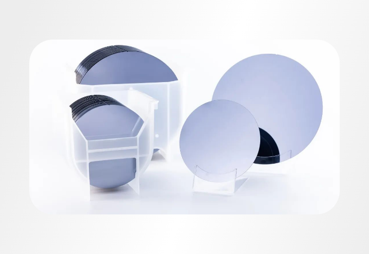
This device adopts ver 2.0 polishing technology can realize one-time polishing of the edges of silicon wafers of various specifications, meeting the polishing requirements of semiconductor grade silicon wafers.
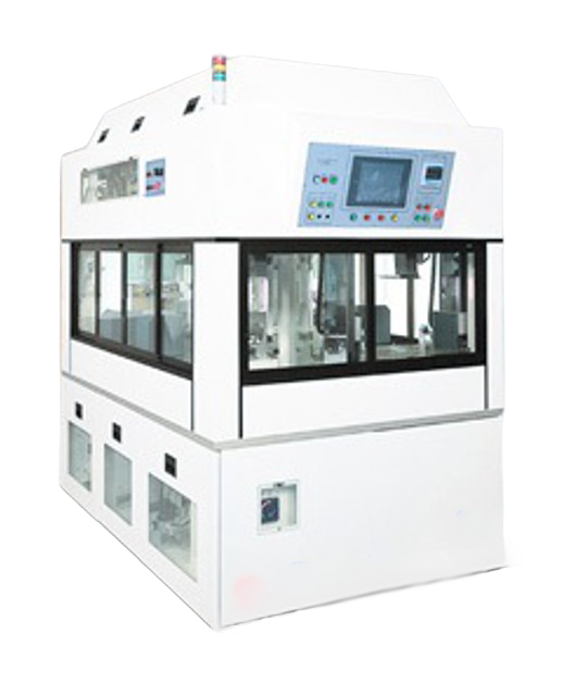
| Item | Description |
|---|---|
| Wafer size | φ100~φ300mm |
| Wafer thickness | 0.7~1.5mm |
| Bevel angle | R,22° |
| VN shape | Semi specification |
| Wafer clamping | Edge clamping type |
| Power | AC 200V, 50/60Hz |
| Basic dimensions | W1900mm × D3220mm × H2350mm |
※For detailed specifications, please contact us

关于产品的咨询及相关事宜,请随时与我们联系。